
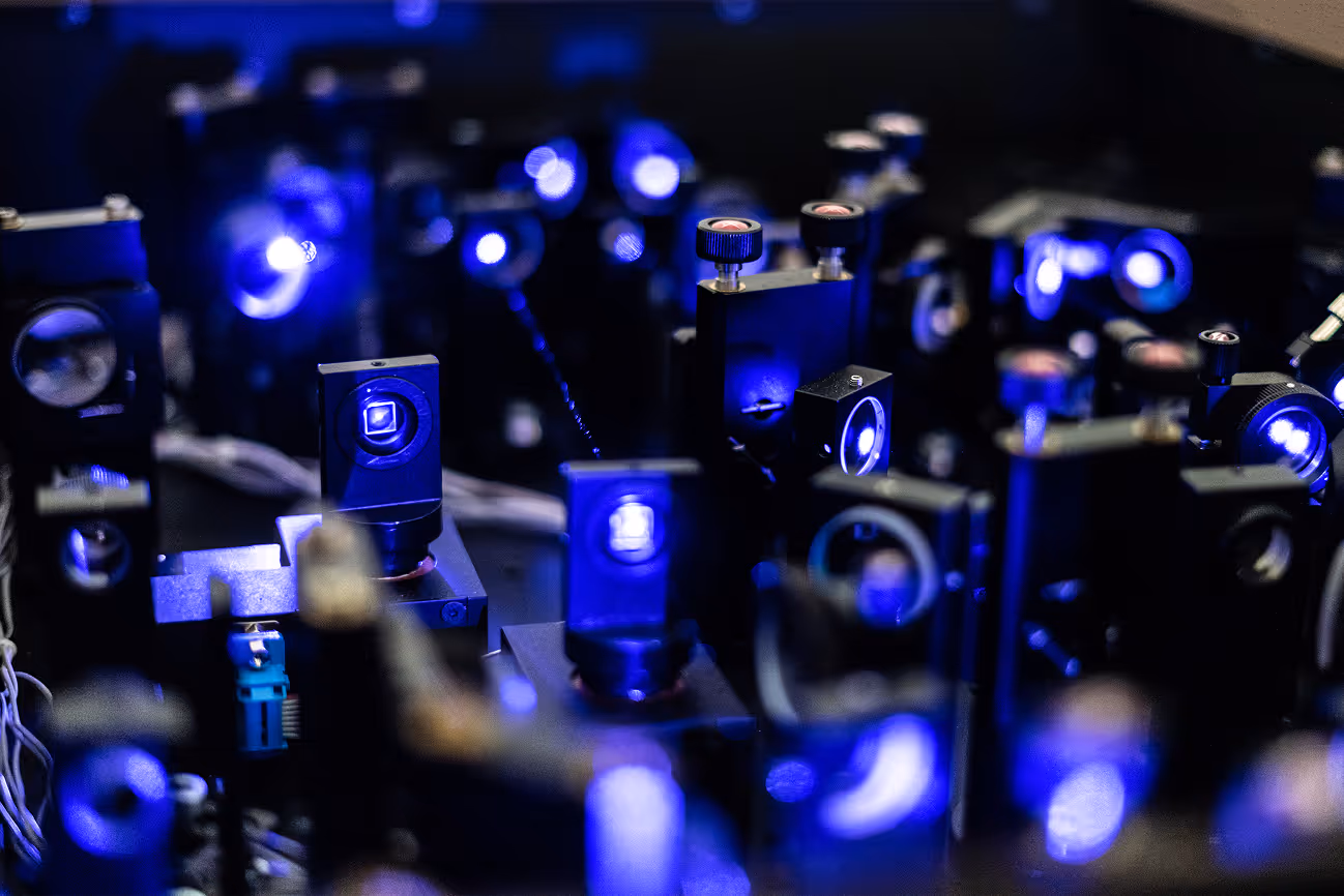
Where Innovation Meets Integration
From materials to manufacturing — scalable SWIR imaging designed for real-world integration


FAQs
Discover answers to common questions about our technology or get in touch today.
SWIR stands for Short-Wave Infrared, typically referring to light in the 900 to 2500 nanometer wavelength range. Unlike visible light, SWIR can see through fog, smoke, silicon, and certain polymers, revealing details invisible to standard optical systems. SWIR enables precise imaging, spectroscopy, and sensing by capturing unique material signatures and temperature-independent contrast.
SWIR is becoming a key performance frontier for next-generation optical systems. Its ability to “see beyond” the visible spectrum opens a wide range of applications including: robotic sensor vision, semiconductor manufacturing, industrial inspection, agriculture quality, medical diagnostics, autonomous vehicle LiDAR, and chemical and biological sensing. These systems demand light sources and detectors that operate efficiently in the SWIR band — a challenge for conventional silicon camera materials.Iris Light’s tunable photonic inks are engineered to address exactly that gap. By enabling on-chip light emission and detection within the SWIR range, we make it possible to design smaller, faster, and more scalable photonic devices — unlocking new capabilities across sectors that rely on precision light control.
While visible imagers are made in the hundreds of billions of units per year due to use of silicon CMOS and favorable wafer-economics, SWIR devices have constrained production volumes due to small wafer formats with relatively exotic production methods. This has resulted in expensive end products and limited deployment. Industrial desire to deeply integrate machine vision with SWIR capability into manufacturing is driving unprecedented demand for higher volume SWIR products. Iris Light’s NanoBLACK™ platform is engineered to address exactly that gap. By enabling wafer-scale integration of SWIR imaging materials directly onto silicon wafers, we make it possible to manufacture SWIR-on-Si sensors, unlocking high-volume manufacturing and enabling new capabilities and markets for SWIR imagers.
Black phosphorus (BP) is a unique semiconductor material made of pure, monoelemental phosphorus. BP possesses a widely tunable direct bandgap ranging from the visible to the mid-infrared (0.3 eV to 2 eV). These various wavelength ranges are accessed by engineering the bulk crystal into two-dimensional (2D) nanosheets known as phosphorene. In contrast, many other 2D semiconductor materials are limited in their spectral window due to indirect bandgaps beyond few-atomic layers. State of the art lasers, LEDS, and photodetectors typically require direct bandgaps to achieve the highest levels of performance.
Iris Light has developed our NanoBLACK™ active photonic nanomaterials to pioneer a new paradigm for integrating direct gap opto-electronic devices into large-scale silicon wafer manufacturing.
If left in ambient without encapsulation, black phosphorus is reactive. However, the same is true of traditional opto-electronic semiconductor materials such as GaAs and InP. In practice, these materials are processed in controlled environments and hermetically packaged. Iris Light incorporates many of these well established techniques to process our nanomaterials, resulting in high-quality devices.