
Novel Nanomaterials Powering the Future of Silicon Photonics and Infrared Imagers
Iris Light is pioneering revolutionary methods for semiconductor manufacturing, including our breakthrough NanoBLACK™ technology. Our mission is to enable scalable manufacturing and widespread deployment of light-based, photonic technologies beyond today’s niche markets.
Advancing Photonics Through Materials Innovation
Iris Light develops photonic inks made of opto-electronically active nanomaterials designed to make light-emitting and detecting components truly integrable with silicon. Our approach simplifies manufacturing while enabling new performance and design possibilities for photonic systems.

National Lab Origins
Deep-Tech Backing
Supported by the U.S. Department of Energy’s Chain Reaction Innovations (CRI) deep-tech entrepreneurship program.
Proven Expertise
Silicon Photonics has long faced bottlenecks when integrating active devices like lasers and long-wavelength photodetectors directly onto silicon. Traditional methods rely on complex bonding and heterogeneous assembly, adding cost, complexity, and limits to scalability. Iris Light’s nanomaterials approach solves this long-standing problem with a completely new approach.
What We Do
We’re pioneering a new class of photonic inks based on opto-electronically active nanomaterials that can be tuned to a variety of ‘colors’ to address the wavelength needs for a diverse set of applications. This simplifies fabrication and opens new pat
Why Choose Us?
Because our photonic inks are process-compatible, they fit into existing manufacturing workflows. That means faster prototyping, higher yields, and easier transition from R&D to production — without reinventing the fab.
Who We are
Iris Light is an Argonne National Lab and Northwestern University spinout, and incubated in the Chain Reaction Innovations (CRI) program sponsored by the Department of Energy. Argonne is one of the nation’s leading science and engineering research centers, known for advancing materials science, nanotechnology, and energy systems at scale. CRI is Argonne’s flagship entrepreneurship program that supports early-stage innovators working to commercialize deep-tech solutions that address critical national challenges. Through CRI, Iris Light gained access to Argonne’s world-class facilities, scientific mentorship, and national lab expertise — helping transition its materials breakthroughs from the research bench to real-world manufacturing.
Our mission is to accelerate the growth and reach of the $2 billion silicon photonics market — driving the next wave of innovation in optical communications, medical devices, autonomous vehicle LiDAR, optical chem-bio sensors, and beyond.
We’re collaborating with end users to define what’s next, systems integrators to prototype it, silicon chip designers to make it, and process engineers to manufacture it. Connect with us! Together we will reimagine the future of what’s possible in photonics.
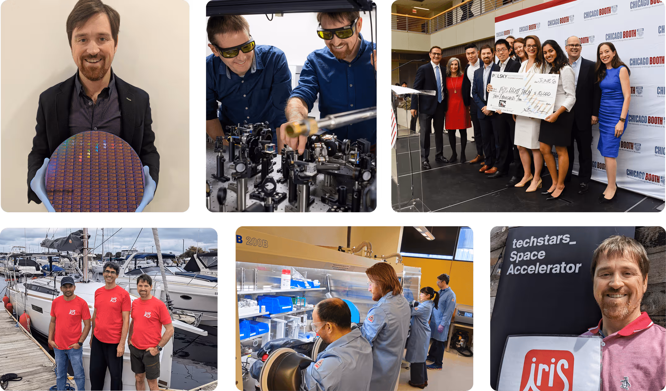
The Iris Light Team
Our team lives at the intersection of research and application. Catch us advancing next-generation photonics in the lab, and sharing NanoBLACK™ with the global photonics community at our next talk.
News from Our Lab
Explore our latest announcements and company updates.


FAQs
Discover answers to common questions about our technology or get in touch today.
SWIR stands for Short-Wave Infrared, typically referring to light in the 900 to 2500 nanometer wavelength range. Unlike visible light, SWIR can see through fog, smoke, silicon, and certain polymers, revealing details invisible to standard optical systems. SWIR enables precise imaging, spectroscopy, and sensing by capturing unique material signatures and temperature-independent contrast.
SWIR is becoming a key performance frontier for next-generation optical systems. Its ability to “see beyond” the visible spectrum opens a wide range of applications including: robotic sensor vision, semiconductor manufacturing, industrial inspection, agriculture quality, medical diagnostics, autonomous vehicle LiDAR, and chemical and biological sensing. These systems demand light sources and detectors that operate efficiently in the SWIR band — a challenge for conventional silicon camera materials.Iris Light’s tunable photonic inks are engineered to address exactly that gap. By enabling on-chip light emission and detection within the SWIR range, we make it possible to design smaller, faster, and more scalable photonic devices — unlocking new capabilities across sectors that rely on precision light control.
While visible imagers are made in the hundreds of billions of units per year due to use of silicon CMOS and favorable wafer-economics, SWIR devices have constrained production volumes due to small wafer formats with relatively exotic production methods. This has resulted in expensive end products and limited deployment. Industrial desire to deeply integrate machine vision with SWIR capability into manufacturing is driving unprecedented demand for higher volume SWIR products. Iris Light’s NanoBLACK™ platform is engineered to address exactly that gap. By enabling wafer-scale integration of SWIR imaging materials directly onto silicon wafers, we make it possible to manufacture SWIR-on-Si sensors, unlocking high-volume manufacturing and enabling new capabilities and markets for SWIR imagers.
Black phosphorus (BP) is a unique semiconductor material made of pure, monoelemental phosphorus. BP possesses a widely tunable direct bandgap ranging from the visible to the mid-infrared (0.3 eV to 2 eV). These various wavelength ranges are accessed by engineering the bulk crystal into two-dimensional (2D) nanosheets known as phosphorene. In contrast, many other 2D semiconductor materials are limited in their spectral window due to indirect bandgaps beyond few-atomic layers. State of the art lasers, LEDS, and photodetectors typically require direct bandgaps to achieve the highest levels of performance.
Iris Light has developed our NanoBLACK™ active photonic nanomaterials to pioneer a new paradigm for integrating direct gap opto-electronic devices into large-scale silicon wafer manufacturing.
If left in ambient without encapsulation, black phosphorus is reactive. However, the same is true of traditional opto-electronic semiconductor materials such as GaAs and InP. In practice, these materials are processed in controlled environments and hermetically packaged. Iris Light incorporates many of these well established techniques to process our nanomaterials, resulting in high-quality devices.